Composable 1RU FPGA application switch combining dual Xilinx UltraScale+ VU9P FPGAs with an integrated 1.5 Tbps L2/L3 switch element for in-network application acceleration at 4-5 ns Layer 1 latency.
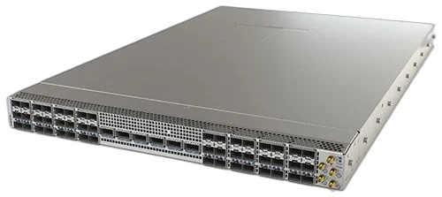
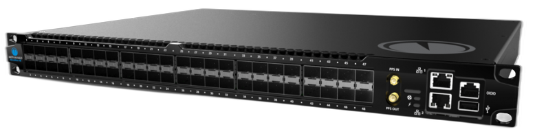
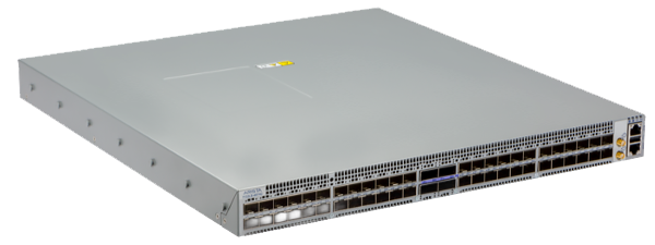
The Arista 7130LBR Series combines two Xilinx UltraScale+ VU9P-3 FPGAs with an integrated R-family merchant-silicon switch element in a single 1RU chassis, targeting deployments where in-network compute (order matching, market data normalisation, risk pre-screening) needs to execute at Layer 1 latency rather than as a separate compute step after forwarding. The FPGA portion of the design provides the reconfigurable logic required to implement custom in-network algorithms in hardware, while the integrated R-family switch delivers 1.5 Tbps of L2/L3 forwarding capacity across 48 SFP+/SFP28 ports and 6 QSFP-DD interfaces, totalling 96 independent 10/25G lanes. The Layer 1 crosspoint carries traffic between ports at 4 nanoseconds on the 10G variant (48S6QD) and 5 nanoseconds on the 25G variant (48S6YD), with the FPGA able to inspect, process, and act on the in-flight data within that forwarding window.
Each FPGA is equipped with 32 GB of DDR4 DRAM, providing the high-bandwidth memory required for table lookups, order book maintenance, and other state-dependent operations that exceed FPGA on-chip BRAM capacity. The 4 GB packet buffer shared across the platform handles burst absorption when the in-network application needs brief additional processing time without dropping packets. The QSFP-DD interfaces support breakout to 2x40GbE or 8x10/25GbE per port, giving the 7130LBR flexible connectivity for both high-density 10/25G access links and 40/100G uplink aggregation within the same 1RU chassis. Two hardware variants address the most common speed requirements: 48S6QD for 10G lane deployments where 4 ns latency is the primary constraint, and 48S6YD for 25G deployments where 5 ns latency across faster lanes is the requirement.
Two VU9P-3 FPGAs operate within the 7130LBR, each connected to its own 32 GB pool of DDR4 DRAM. The dual-FPGA configuration allows the processing workload to be split between two independent reconfigurable compute elements (for example, one FPGA handling order book state maintenance for exchange A while the second handles normalisation for exchange B) without the FPGAs competing for shared memory bandwidth. The UltraScale+ architecture provides the logic cell density and DSP slice count required for algorithms that would be too large for earlier FPGA generations, and the VU9P speed grade provides the timing margin needed to implement logic that must complete within the 4-5 ns Layer 1 forwarding window. Applications are deployed as bitstream files that reconfigure the FPGA fabric without disrupting the Layer 1 switch element.
The 7130LBR supports native one-to-many connectivity at the Layer 1 crosspoint, allowing a single input stream to be replicated to multiple outputs simultaneously without additional tap hardware. In market data distribution environments where a single exchange feed must be delivered to dozens of co-located trading engines simultaneously, 1:N replication at Layer 1 ensures all recipients receive identical copies of the data at the same deterministic latency, rather than through a Layer 2 multicast mechanism that introduces variable forwarding delay depending on queue occupancy at the time of replication. The integrated R-family switch element handles the L2/L3 forwarding for traffic that requires standard Ethernet switching, while the Layer 1 crosspoint handles the latency-critical replication paths; both functions coexist in the same chassis.
The 48 SFP+/SFP28 ports and 6 QSFP-DD interfaces combine to provide 96 independent 10/25G lanes within a single 1RU chassis. The QSFP-DD interfaces support breakout to either 2x40GbE or 8x10/25GbE per port, which means the 6 QSFP-DD ports can contribute up to 48 additional 10/25G lanes beyond the 48 SFP+ ports when configured for maximum density. This port density allows the 7130LBR to serve as a top-of-rack Layer 1 and FPGA compute element for a full rack of servers without requiring a separate switch chassis, reducing the number of distinct rack units required for the Layer 1 switching, FPGA processing, and server connectivity functions that would otherwise occupy separate 1RU devices per function.
The R-family switch element integrated into the 7130LBR provides full L2/L3 forwarding at 1.5 Tbps, a dedicated switching capacity separate from the FPGA processing paths. This integration means the 7130LBR can simultaneously handle both the deterministic Layer 1 forwarding required for latency-critical paths and standard Ethernet switching for management, control, and monitoring traffic, without requiring a separate upstream switch. Traffic flows that do not require FPGA processing are handled directly by the R-family switch at standard Ethernet forwarding speeds, while flows that require FPGA inspection traverse the Layer 1 crosspoint. The 4 GB packet buffer associated with the switch element absorbs traffic bursts that arrive faster than downstream capacity can accept, protecting against packet loss during momentary congestion.
Full specifications for Arista 7130LBR Series
Download product documentation and resources
Explore other configurations and models that might suit your needs.
Recommended
#Arista-7130S-1
Recommended
#DCS-7130-48LS-F
Recommended
#DCS-7132LB-48Y4C
Our team of experts is ready to help you find the perfect solution for your business needs. Get personalized advice and competitive quotes.
We're here to help with any questions